Creating PCB artwork
This page will help you create suitable circuit artwork for single or double sided prototype circuit boards to use with your projects.
I use Altium Designer for all my projects as it makes it possible to follow the design from an idea through to a working prototype. The process has few basic steps: Initial Idea -> Schematic Capture and Code development -> PCB layout and routing -> Manufacture.
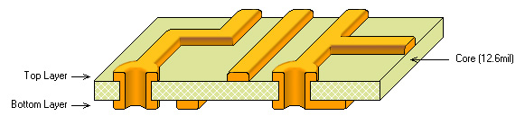
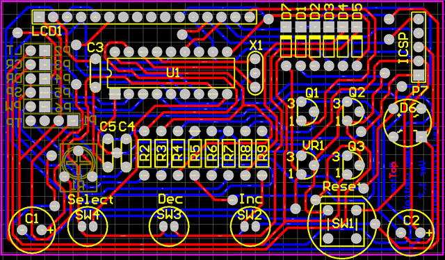
Once you have created a schematic diagram of your project you are ready to export Netlist in to a PCB document. Doing so will automatically create all necessary component footprints and logical connections on a blank PCB document (refer to the picture on left). The next step is to move the component footprints around to comply with your PCB size and shape making sure component heights have no contentions. In the picture to the left most components are underneath the LCD. This process is called PCB Layout.
Step 1 - Component Layout.
Step 2 - Defining PCB type.
Most PCB routing software can allow multiple routing layers, some up to 16. However creating a multi layer PCB of more than 2 layers is not possible without professional gear. For home made prototypes 1 or 2 layer PCB will suffice. You need to tell the software that the PCB is a 1 or 2 layer PCB.
Step 3 - Defining Routing Rules.
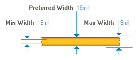
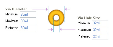
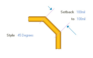
Next you need to define some rules which the routing software will follow. The values in the pictures on the left are minimum values that will produce an artwork which is easily transferable on to PCB. If you decide to use smaller sizes and clearances you may run in to problems of broken tracks or tracks shorting during the transfer process. This step is the most important one for successful and hustle free PCB manufacture. You may experiment with different values if you need to adjust clearances and sizes on some projects but I would try to stick as close to these values as possible. If the PCB size allows greater sizes and widths then feel free to adjust as needed. I tend to make my POWER tracks (GND and V+) thicker than signal tracks.
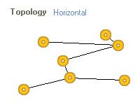
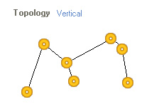
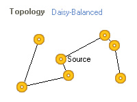
Step 4 - Defining Routing Topology .
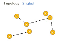
Routing topology is a rule that determines how the router will interpret netlist connections on a given PCB component layout. This only comes in to play when designing crucial timing PCBs. I generally use topology called "Shortest". This is sufficient for most projects and minimizes the number of vias on the circuit board.
Step 5 - Routing and Cleanup.
Once all above steps have been completed to your satisfaction it is time to start auto routing and make a cup of coffee. Depending on PCB complexity and the speed of your PC this may take from few seconds to many minutes. During routing the software will run through few passes using different strategies (depending on which software you use). You may choose to re-route few times making small adjustments to component layout and routing rules. The key is to end up with as few vias as possible if your design is double-sided. When you are satisfied with the routed document you need to zoom in and manually clean up redundant bits of track and manually re-route some connections as you see fit.
The great thing about auto route is that it does most of the bulk work for you, however it is not smart enough to clean up all redundant tracks, that is why you need to do this manually. You also need to make sure that all vias are not underneath any components. This is the most time consuming step but if you are like me and like to have the board looking nice and neat then it is a small price to pay.
Step 6 - Printing the artwork .
The last step in the process is printing the artwork on to transfer film. Because transfer film is not that cheap I would suggest printing on to a normal paper first to get all settings correct. You need to remember that the top artwork is printed in MIRROR mode where as the bottom is printed as is. Things to check before printing are: Orientation, Scaling = OFF, Page Size, etc. Once you are happy with all settings, printout both sides on plain paper. Place the two sheets together (toner touching) and check if all pads align correctly over a lamp or holding the pages up to light. When you are happy with the result you may print on to transfer film.